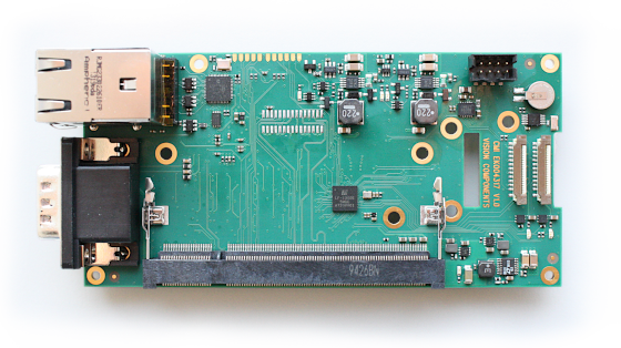
VC Compute Module Interface Board
Hardware specifications of the VC CMI Board for the use with Raspberry Pi Compute Module 3/3+
| Revision: | 0.13 |
|---|---|
| Date: | 2020-04-28 |
| Contact: | support@vision-comp.com |
| Copyright: | 2020 Vision Components GmbH Ettlingen, Germany |
| Author: | VC Support, mailto:support@vision-comp.com |
This documentation has been prepared with most possible care. However Vision Components GmbH does not take any liability for possible errors. In the interest of progress, Vision Components GmbH reserves the right to perform technical changes without further notice.
Please notify support@vision-components.com if you become aware of any errors in this manual or if a certain topic requires more detailed documentation.
This manual is intended for information of Vision Component’s customers only. Any publication of this document or parts thereof requires written permission by Vision Components GmbH.
| Symbol | Meaning |
|---|---|
 |
The Light bulb highlights hints and ideas that may be helpful for a development. |
 |
This warning sign alerts of possible pitfalls to avoid. Please pay careful attention to sections marked with this sign. |
 |
This is a sign for an example. |
Trademarks
Linux, Debian, the Tux logo, Vivado, Xilinx and Zynq, ARM, Cortex, Windows XP, Total Commander, Tera Term, Motorola, HALCON, Vision Components are registered Trademarks. All trademarks are the property of their respective owners.
Raspberry Pi and Raspbian are also registered Trademarks. All trademarks are the property of their respective owners.
Table of Contents
1 General Information
The VC Compute Module Interface Board (CMI) is designed for a RaspberryPi CM3 Compute Module and CM3+. It has two MIPI connectors for connecting camera sensors. There are pins for triggering the image sensors and flash output pins with configurable current where several Power LEDs may be driven directly. The board features mounting options for our LED flash rings and camera sensors. Moreover it features an ethernet socket and an USB port as well as four PLC input and output lanes. There is also an Micro-SD card slot and a real time clock (RTC). A FPGA for managing triggering/flashing and input/output mappings is pre-programmed, but can also be reprogrammed directly by the customer.
2 Technical Specifications
| Component / Feature | Specification |
|---|---|
| Dimensions | 125 x 57 x 30 mm (without mounting LED ring) |
| Trigger input | Opto-isolated, 8 mA @ 5 V |
| Process interface | PLC: 4 inputs / 4 outputs, outputs 4×200 mA, FPGA IO: 4 Digital LVCMOS (3.3 V) GPIOs |
| Trigger | 1 flash trigger output at 24 V, 1 trigger input |
| LED driver | 2 LED driver outputs (1 shared with flash trigger output) |
| Ethernet interface | 1000 Mbit/s |
| Serial interface | Available as RS-232 interface |
| Storage Conditions | Temperature: -20 to +60 °C, Max. humidity: 90%, non condensing. |
| Operating Conditions | Temperature: 0 to +50 °C, Max. humidity: 80%, non condensing. |
| Nominal voltage Vdd for power supply | 12–24 V DC |
| Nominal Power consumption | 12 W (max, dependent on many things like hardware connected over USB, Flash LEDs, etc.) not including PLC outputs |
3 Hardware Interfaces

VC CMI socket overview (Top view)
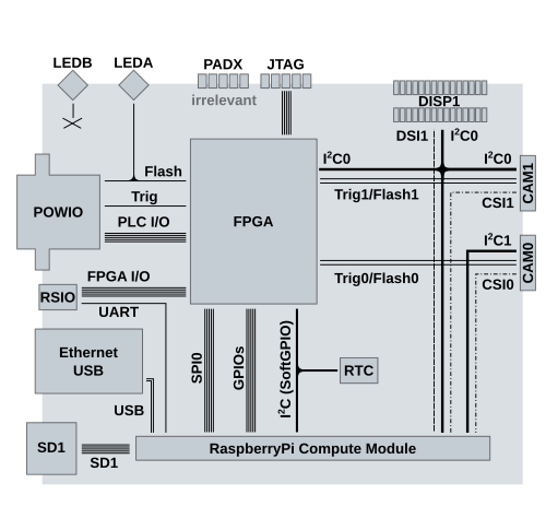
VC CMI block diagram
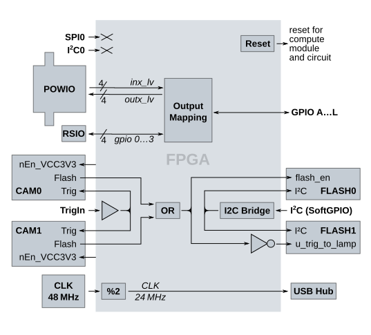
VC CMI default FPGA block diagram
3.1 Power, Trigger and PLC Connector POWIO
| CMI Socket Frontal View | Pin | Signal | Level |
|---|---|---|---|
 |
1 | Main Power Supply | Vdd |
| 2 | Common Ground | GND | |
| 3 | PLC In0 | +5–24 V | |
| 4 | PLC Out0 | Vdd | |
| 5 | PLC In1 | +5–24 V | |
| 6 | PLC Out1 | Vdd | |
| 7 | PLC Out2 | Vdd | |
| 8 | PLC In2 | +5–24 V | |
| 9 | PLC Out3 | Vdd | |
| 10 | PLC In3 | +5–24 V | |
| 11 | FLASH0 | Vdd 0–1.5 A | |
| 12 | FLASH1 | Vdd 0–1.5 A | |
| 13 | N/C | — | |
| 14 | TrigIn_P | +5 V | |
| 15 | TrigIn_M | GND |
All inputs are 5–24 V, 2.4 mA @ 5 V and 5 mA @ 24 V, 200 kHz max., threshold: positive +1.3 mA typ., negative 0.7 mA typ.
3.1.1 POWIO PLC IOs
| Separation of PLC/trigger output voltage | PLC outputs supply not separated from power supply |
| PLC Input Voltage | Identical with power supply voltage |
| PLC Input Current (max) | 2.4 mA @ 5 V and 5 mA @ 24 V, 200 kHz max., threshold: positive +1.3 mA typ., negative 0.7 mA typ. |
| PLC Output Voltage | Identical with power supply Voltage — internally connected |
| PLC Output Current (max) | 4 × 200 mA Max total of all outputs: 0.8 A |
| Max Current for 1 Power / PLC connector pin | 200 mA |
| Power failure detection | Poly Fuse |
The maximum combined current of all outputs should not exceed 1 A.
3.1.2 POWIO Trigger Input
| Separation of trigger input | Yes, optically isolated, 8 mA @ 5 V |
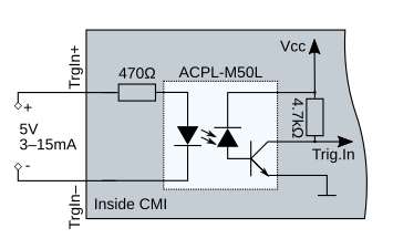
Connection of Trigger Input
3.1.3 POWIO/LED A Flash Output
The Hardware features two independently adjustable current sources for the connection of two LED light sources. They are designed for controlling the ring illuminators around the lens, connected to LED A. They are also accessible over the connector POWIO.
The controller covers a current range from 150 to 1500 mA.
The duty cycle is limited to 1:8, i.e. the off-state is eight times longer than the on-state for the output. Example: 1 ms flash duration, 8 ms cool down duration.
The default FPGA has a protection which limits the maximum flash duration to 2 ms. This is to protect LEDs which cannot support 1.5 A over a longer time period. For developping own LED rings, there is also an analogue protection at FLASH1 while the FLASH0 can theoretically support 1.5 A steady (please note, that this current is not calculated to the nominal power consumption).
| Iout | 150–1500 mA, programmable |
| Uout | 4–16 V (1–4 LEDs in series depending on the Vf) |
Warning
Do not connect inductive loads to FLASH0 or FLASH1 outputs!
Note
The default FPGA limits the maximum flash duration to 2 ms of both flash outputs for LED protection,
while FLASH1 is additionally limited by a slower analogue protection circuit.
FLASH0 and FLASH1 behave different: While the FLASH0 output can be used for triggering, the FLASH1 output is not intended for triggering external flash!
FLASH1 has a small steady current flow for providing an instant power supply. This may lead to dark glimming LEDs connected to the FLASH1 output while LEDs connected to the FLASH0 output won't emit light (i.e. one half of a VC LED ring would glow).
3.1.3.1 Connection of Flash Outputs: External Flash
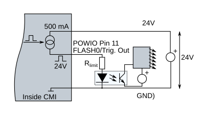
Connection of Flash Outputs using an external Flash Current Source and Opto-Isolation
The figure shows how to connect an external flash illumination to FLASH0/TrigOut signal by using an opto isolation. R limit should be chosen to protect the opto isolator, e.g. 2K2/250 mW for a current of 10 mA. Remark: R limit is not necessary for Vision Components' High Power IR Illumination (VK002180). The current source should be set to 500 mA.
FLASH1 output is not intended for triggering an external flash!
3.1.3.2 Connection of Flash Outputs: Direct High-Power-LEDs

Connection of Flash Outputs directly to High-Power LEDs
The figure shows how to connect an external flash illumination. The current source should be set to the required current setting between 200 and 1500 mA. The time limit must be set to an appropriate value for the protection of the LEDs according to the data sheet of the manufacturer. Connectable are 1 to 6 High Power LEDs.
3.1.3.3 Connection of Flash Outputs: PLC
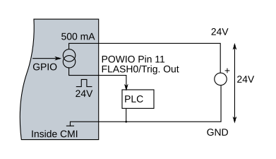
Connection of Flash Outputs to a PLC
The figure shows how to connect a PLC to the FLASH0/TrigOut or FLASH1 signal. The current source should be set to 500 mA.
FLASH1 output is not intended for triggering an external flash!
3.1.3.4 Connection of LED Rings over LED A: Internal Flash
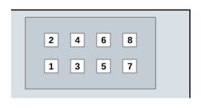
| Camera Socket Top View | Pin | LED A Signal | LED B Signal |
|---|---|---|---|
 |
1 | GND | GND |
| 2 | N/C | N/C | |
| 3 | FLASH0 | N/C | |
| 4 | FLASH1 | N/C |
The current source should be set to the required current setting between 200 and 1500 mA. The time limit must be set to an appropriate value for the protection of the LEDs according to the data sheet of the manufacturer.
Warning
Be careful not to produce a short circuit between the VC MIPI sensor (which has a grounded surface) and the LED ring!
3.2 RS-232 and FPGA IO Connector RSIO
A FPGA IO connects to the onboard FPGA which itself may also be programmed to have connections to some RaspberryPi GPIOs.
| Camera Socket Top View | Pin | Signal | Additional Information |
|---|---|---|---|
 |
1 | V24_TxD | Native RS-232 interface |
| 2 | +3.3 V | — | |
| 3 | V24_RxD | Native RS-232 interface | |
| 4 | FPGA IO 1 | Digital LVCMOS (3.3 V) | |
| 5 | GND | — | |
| 6 | FPGA IO 2 | Digital LVCMOS (3.3 V) | |
| 7 | FPGA IO 0 | Digital LVCMOS (3.3 V) | |
| 8 | FPGA IO 3 | Digital LVCMOS (3.3 V) |
Note
FPGA IO signals are LVCMOS 3.3 V.
Warning
The FPGA IO I/Os are very sensitive (also to ESD) and not
galvanically separated. Opto-isolation of the driving circuit is
therefore strongly recommended. It is also recommended to keep the cable
as short as possible!
The I/Os are not protected against over current. The I/Os are neither protected against short circuit nor reverse voltage spikes from inductive loads.
Be careful: Reversing the connector is not allowed and may damage the board!
3.3 The CAM0 Socket
Note
The RaspberryPi Naming for the camera interfaces CAM?_… are represented at this document by the more generic ones CSI?_… (camera serial interface).
The CAM0 Socket connects to CSI0 but to I2C1 for compatibility. The CAM0 Socket only supports 2 MIPI data lanes in contrast to the CAM1 socket with 4 lanes.
Beneath the CAM0 socket is a LED which emits green light if the CAM0 socket is powered.
| Camera Socket | Pin | Signal |
|---|---|---|
 |
1 | +3.3 V |
| 2 | I2C1 SDA | |
| 3 | I2C1 SCL | |
| 4 | GND | |
| 5 | FPGA CAM0 FLASH | |
| 6 | FPGA CAM0 TRIG | |
| 7 | GND | |
| 8 | N/C | |
| 9 | N/C | |
| 10 | GND | |
| 11 | N/C | |
| 12 | N/C | |
| 13 | GND | |
| 14 | CSI0 CP | |
| 15 | CSI0 CN | |
| 16 | GND | |
| 17 | CSI0 DP1 | |
| 18 | CSI0 DN1 | |
| 19 | GND | |
| 20 | CSI0 DP0 | |
| 21 | CSI0 DN0 | |
| 22 | GND |
3.4 The CAM1 Socket
The CAM1 socket connects to CSI1 but to I2C0 for compatibility. Only this Socket supports 4 MIPI data lanes.
Beneath the CAM1 socket is a LED which emits green light if the CAM1 socket is powered.
| Camera Socket | Pin | Signal |
|---|---|---|
|
1 | +3.3 V |
| 2 | I2C0 SDA | |
| 3 | I2C0 SCL | |
| 4 | GND | |
| 5 | FPGA CAM1 FLASH | |
| 6 | FPGA CAM1 TRIG | |
| 7 | GND | |
| 8 | CSI1 DP3 | |
| 9 | CSI1 DN3 | |
| 10 | GND | |
| 11 | CSI1 DP2 | |
| 12 | CSI1 DN2 | |
| 13 | GND | |
| 14 | CSI1 CP | |
| 15 | CSI1 CN | |
| 16 | GND | |
| 17 | CSI1 DP1 | |
| 18 | CSI1 DN1 | |
| 19 | GND | |
| 20 | CSI1 DP0 | |
| 21 | CSI1 DN0 | |
| 22 | GND |
3.5 Display Interface Connector DISP1
The DISP1 Socket connects to DSI1 but to I2C0 for compatibility.
| Display Socket Top View | Pin | Signal |
|---|---|---|
 |
1 | GND |
| 2 | DSI1 DN1 | |
| 3 | DSI1 DP1 | |
| 4 | GND | |
| 5 | DSI1 CN | |
| 6 | DSI1 CP | |
| 7 | GND | |
| 8 | DSI1 DN0 | |
| 9 | DSI1 DP0 | |
| 10 | GND | |
| 11 | I2C0 SCL | |
| 12 | I2C0 SDA | |
| 13 | GND | |
| 14 | +3.3 V | |
| 15 | +3.3 V | |
| 16–30 | N/C |
The display itself needs the dt-blob.bin generated from the dt-blob.dts and copied into the /boot (not /boot/overlays) directory.
Note
The touchscreen functionality of the raspberrypi display disturbs the I²C communication with CAM1, so be sure to have turned it off by adding the following command to your /boot/config.txt:
disable_touchscreen=1
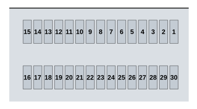
3.6 RaspberryPi Compute Module Connector
3.6.1 RaspberryPi GPIO Connections
| GPIO-Nr. | Direction | Connects to |
|---|---|---|
| GPIO 0 | I/O | I2C0 SDA |
| GPIO 1 | I/O | I2C0 SCL |
| GPIO 2 | I/O | I2C1 SDA |
| GPIO 3 | I/O | I2C1 SCL |
| GPIO 4 | I/O | FPGA RPI GPIO A |
| GPIO 5 | I/O | FPGA RPI GPIO B |
| GPIO 6 | I/O | FPGA RPI GPIO C |
| GPIO 7 | I/O | FPGA RPI GPIO D |
| GPIO 8 | I/O | FPGA SPI0 CE0 N |
| GPIO 9 | I/O | FPGA SPI0 MISO |
| GPIO 10 | I/O | FPGA SPI0 MOSI |
| GPIO 11 | I/O | FPGA SPI0 SCLK |
| GPIO 12 | I/O | FPGA RPI GPIO E |
| GPIO 13 | I/O | FPGA RPI GPIO F |
| GPIO 14 | I/O | RSIO V24_TxD |
| GPIO 15 | I/O | RSIO V24_RxD |
| GPIO 16 | I/O | FPGA RPI GPIO G |
| GPIO 17 | I/O | FPGA RPI GPIO H |
| GPIO 18 | I/O | FPGA RPI GPIO I |
| GPIO 19 | I/O | FPGA RPI GPIO J |
| GPIO 20 | I/O | FPGA RPI GPIO K |
| GPIO 21 | I/O | FPGA RPI GPIO L |
| GPIO 22 | N/C | — |
| GPIO 23 | I/O | FPGA I2C SDA |
| GPIO 24 | I/O | FPGA I2C SCL |
| GPIO 25 | N/C | — |
| GPIO 26 | N/C | — |
| GPIO 27 | N/C | — |
| GPIO 28 | INPUT | PULLDOWN |
| GPIO 29 | INPUT | PULLDOWN |
| GPIO 30 | N/C | — |
| GPIO 31 | N/C | — |
| GPIO 32 | N/C | — |
| GPIO 33 | N/C | — |
| GPIO 34 | I/O | SD1 CLK |
| GPIO 35 | I/O | SD1 CMD |
| GPIO 36 | I/O | SD1 DAT0 |
| GPIO 37 | I/O | SD1 DAT1 |
| GPIO 38 | I/O | SD1 DAT2 |
| GPIO 39 | I/O | SD1 DAT3 |
| GPIO 40 | I/O | SD1 DAT4 |
| GPIO 41 | I/O | SD1 DAT5 |
| GPIO 42 | I/O | SD1 DAT6 |
| GPIO 43 | I/O | SD1 DAT7 |
| GPIO 44 | INPUT | PULLDOWN |
| GPIO 45 | INPUT | PULLDOWN |
3.6.2 RaspberryPi USB Connections
The Pins USB DP and USB DM connect to an USB hub with two devices attached:
- Gigabit Ethernet, and
- the USB socket.
The hub is driven by a 24 MHz clock by the default FPGA.
3.7 Real Time Clock
The Maxim DS1374 RTC is connected to the FPGA I2C bus. It is accessible over address 0x68. An accumulator which buffers the RTC must be activated to be charged: The only allowed values for register 0x09 to be written are 0xaa for charging, and 0x00.
Warning
Writing values to register 0x09 different from 0xaa or 0x00 is not allowed and may damage the board!
Example
This is a low-level approach as root.
We assume the RTC is already detected as 0x68 at I2C bus 3, check with:
i2cdetect 3
beforehand. This sequence should activate charging:
modprobe -r rtc_ds1374
i2ctransfer -y 3 w2@0x68 0x09 0xaa
i2ctransfer -y 3 w1@0x68 0x09 r1@0x68
modprobe rtc-ds1374
hwclock --systohc
hwclock -r
3.8 JTAG Connector
The JTAG connector is the JTAG interface for programming the onboard FPGA.
| Camera Socket Top View | Pin | Signal |
|---|---|---|
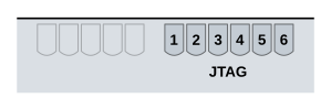 |
1 | +3.3 V |
| 2 | FPGA TCK | |
| 3 | FPGA TDI | |
| 4 | FPGA TDO | |
| 5 | FPGA TMS | |
| 6 | GND |
Information about programming the FPGA is covered in an extra document.
4 FPGA Setup
A default FPGA circuit is factory pre-programmed.
It has the following behaviour:
- Powers up both mipi sockets,
- Provides a 24 MHz clock for the USB hub which connects Ethernet and the USB port to the RaspberryPI,
- Common resetting functionality for the compute module itself (signal run) and for the rest of the board,
- Redirection of the POWIO TrigIn signal to both mipi modules,
- Redirection of both mipi module flash signals to both FLASH0 and FLASH1,
- Digital protection of FLASH0 and FLASH1 by limiting the flash output duration to 2 ms.
- Redirection of FPGA RPI GPIO A … FPGA RPI GPIO D to PLC Out0 … PLC Out3, which effectively connects GPIO 4 … GPIO 7 with PLC Out0 … PLC Out3.
Information about programming the FPGA is covered in an extra document.
5 Software Setup
For the following we assume you are using Raspbian Buster.
Note
This hardware does not support flashing data on a RaspberryPi compute module. It has to be done, for example, with a RaspberryPi CM3IO board.
Be sure to enable UART at the /boot/config.txt and SSH remote access for being able to use it on the interface board.
5.1 Preparation
For using the RaspberryPi Compute Module at the VC CMI board, it has to be flashed beforehand with a Raspbian Buster image.
At the time of writing, Raspbian Buster has neither enabled the UART interface, nor the SSH remote access. This means, that you cannot login to your system without prior modification of the /boot/config.txt (UART) and/or activation of the SSH server (raspi-config).
For activation of the UART, and thus the RS232 interface at RSIO, add the following line to your /boot/config.txt:
dtoverlay=uart0
For activation of the SSH server, start the raspi-config program by running the following command:
sudo raspi-config
Then select Interfacing Options, then SSH and agree the question whether to enable the SSH server with <Yes>, leave the program.
5.2 Driver Installation
There is a DKMS driver as Debian package available for the VC MIPI modules which include the setup for the CMI GPIOs. Please visit our website to get it.
Debian packages can be installed by using the command dpkg -i.
5.3 GPIO Software Setup
Not mentioned GPIOs may use their default function.
| GPIO-Nr. | Selector | Becomes | Why |
|---|---|---|---|
| GPIO 0 | ALT 0 | I2C0_SDA | Communication with CAM1 |
| GPIO 1 | ALT 0 | I2C0_SCL | Communication with CAM1 |
| GPIO 2 | ALT 0 | I2C1_SDA | Communication with CAM0 |
| GPIO 3 | ALT 0 | I2C1_SCL | Communication with CAM0 |
| GPIO 4 | OUTPUT | OUTPUT | Access to PLC Out0 [1] |
| GPIO 5 | OUTPUT | OUTPUT | Access to PLC Out1 [1] |
| GPIO 6 | OUTPUT | OUTPUT | Access to PLC Out2 [1] |
| GPIO 7 | OUTPUT | OUTPUT | Access to PLC Out3 [1] |
| GPIO 8 | ALT 0 | SPIO0_CE0_N | SPI utilisation at FPGA |
| GPIO 9 | ALT 0 | SPIO0_MISO | SPI utilisation at FPGA |
| GPIO 10 | ALT 0 | SPIO0_MOSI | SPI utilisation at FPGA |
| GPIO 11 | ALT 0 | SPIO0_SCLK | SPI utilisation at FPGA |
| GPIO 12 | INPUT | INPUT | Access to PLC In0 [1] |
| GPIO 13 | INPUT | INPUT | Access to PLC In1 [1] |
| GPIO 14 | ALT 0 | UART0_TX | RS-232 access over RSIO |
| GPIO 15 | ALT 0 | UART0_RX | RS-232 access over RSIO |
| GPIO 16 | INPUT | INPUT | Access to PLC In2 [1] |
| GPIO 17 | INPUT | INPUT | Access to PLC In3 [1] |
| GPIO 18 | OUTPUT | OUTPUT | Access to FPGA IO 0 over RSIO [1] |
| GPIO 19 | OUTPUT | OUTPUT | Access to FPGA IO 1 over RSIO [1] |
| GPIO 20 | INPUT | INPUT | Access to FPGA IO 2 over RSIO [1] |
| GPIO 21 | INPUT | INPUT | Access to FPGA IO 3 over RSIO [1] |
| GPIO 23 | INPUT | INPUT | Soft-I2C3 to RTC and Flash current setting [1] |
| GPIO 24 | INPUT | INPUT | Soft-I2C3 to RTC and Flash current setting [1] |
| ⋮ | — | — | GPIO 25–GPIO 37 unused |
| GPIO 28 | INPUT | INPUT | externally pulled down |
| GPIO 29 | INPUT | INPUT | externally pulled down |
| ⋮ | — | — | GPIO 30–GPIO 33 unused |
| GPIO 34 | ALT 3 | SD1_CLK | Access to Micro-SD card slot |
| GPIO 35 | ALT 3 | SD1_CMD | Access to Micro-SD card slot |
| GPIO 36 | ALT 3 | SD1_DAT0 | Access to Micro-SD card slot |
| GPIO 37 | ALT 3 | SD1_DAT1 | Access to Micro-SD card slot |
| GPIO 38 | ALT 3 | SD1_DAT2 | Access to Micro-SD card slot |
| GPIO 39 | ALT 3 | SD1_DAT3 | Access to Micro-SD card slot |
| GPIO 40 | ALT 3 | SD1_DAT4 | Access to Micro-SD card slot |
| GPIO 41 | ALT 3 | SD1_DAT5 | Access to Micro-SD card slot |
| GPIO 42 | ALT 3 | SD1_DAT6 | Access to Micro-SD card slot |
| GPIO 43 | ALT 3 | SD1_DAT7 | Access to Micro-SD card slot |
| [1] | (1, 2, 3, 4, 5, 6, 7, 8, 9, 10, 11, 12, 13, 14) at least if using the default FPGA. |
GPIO in- and outputs can be accessed over the linux standard way via /sys/class/gpio, see: https://www.kernel.org/doc/Documentation/gpio/sysfs.txt
You may install the program named raspi-gpio by executing:
sudo apt install raspi-gpio
See the help text of the program how to change the function of the GPIOs. A good output will look like this:
BANK0 (GPIO 0 to 27):
GPIO 0: level=1 fsel=4 alt=0 func=SDA0
GPIO 1: level=1 fsel=4 alt=0 func=SCL0
GPIO 2: level=1 fsel=4 alt=0 func=SDA1
GPIO 3: level=1 fsel=4 alt=0 func=SCL1
GPIO 4: level=0 fsel=1 func=OUTPUT
GPIO 5: level=0 fsel=1 func=OUTPUT
GPIO 6: level=0 fsel=1 func=OUTPUT
GPIO 7: level=0 fsel=1 func=OUTPUT
GPIO 8: level=1 fsel=4 alt=0 func=SPI0_CE0_N
GPIO 9: level=0 fsel=4 alt=0 func=SPI0_MISO
GPIO 10: level=0 fsel=4 alt=0 func=SPI0_MOSI
GPIO 11: level=0 fsel=4 alt=0 func=SPI0_SCLK
GPIO 12: level=1 fsel=0 func=INPUT
GPIO 13: level=1 fsel=0 func=INPUT
GPIO 14: level=1 fsel=4 alt=0 func=TXD0
GPIO 15: level=1 fsel=4 alt=0 func=RXD0
GPIO 16: level=1 fsel=0 func=INPUT
GPIO 17: level=1 fsel=0 func=INPUT
GPIO 18: level=0 fsel=1 func=OUTPUT
GPIO 19: level=0 fsel=1 func=OUTPUT
GPIO 20: level=0 fsel=0 func=INPUT
GPIO 21: level=0 fsel=0 func=INPUT
GPIO 22: level=0 fsel=0 func=INPUT
GPIO 23: level=1 fsel=0 func=INPUT
GPIO 24: level=1 fsel=0 func=INPUT
GPIO 25: level=0 fsel=0 func=INPUT
GPIO 26: level=0 fsel=0 func=INPUT
GPIO 27: level=0 fsel=0 func=INPUT
BANK1 (GPIO 28 to 45):
GPIO 28: level=0 fsel=0 func=INPUT
GPIO 29: level=0 fsel=0 func=INPUT
GPIO 30: level=0 fsel=0 func=INPUT
GPIO 31: level=0 fsel=0 func=INPUT
GPIO 32: level=0 fsel=0 func=INPUT
GPIO 33: level=0 fsel=0 func=INPUT
GPIO 34: level=0 fsel=7 alt=3 func=SD1_CLK
GPIO 35: level=1 fsel=7 alt=3 func=SD1_CMD
GPIO 36: level=1 fsel=7 alt=3 func=SD1_DAT0
GPIO 37: level=1 fsel=7 alt=3 func=SD1_DAT1
GPIO 38: level=1 fsel=7 alt=3 func=SD1_DAT2
GPIO 39: level=1 fsel=7 alt=3 func=SD1_DAT3
GPIO 40: level=1 fsel=7 alt=3 func=SD1_DAT4
GPIO 41: level=1 fsel=7 alt=3 func=SD1_DAT5
GPIO 42: level=1 fsel=7 alt=3 func=SD1_DAT6
GPIO 43: level=1 fsel=7 alt=3 func=SD1_DAT7
GPIO 44: level=0 fsel=0 func=INPUT
GPIO 45: level=0 fsel=0 func=INPUT
BANK2 (GPIO 46 to 53):
GPIO 46: level=1 fsel=0 func=INPUT
GPIO 47: level=1 fsel=1 func=OUTPUT
GPIO 48: level=0 fsel=4 alt=0 func=SD0_CLK
GPIO 49: level=1 fsel=4 alt=0 func=SD0_CMD
GPIO 50: level=1 fsel=4 alt=0 func=SD0_DAT0
GPIO 51: level=1 fsel=4 alt=0 func=SD0_DAT1
GPIO 52: level=1 fsel=4 alt=0 func=SD0_DAT2
GPIO 53: level=1 fsel=4 alt=0 func=SD0_DAT3
5.4 Setting Flash Currents
At the default setup of the FPGA the flash output controller is accessable over the I2C Soft-GPIO. The value to write is calculated by the following formula:
val = (Iout * 192 / 1500) << 4
The I²C flash controller does not have register addresses, so submit the desired value using an I2C block write to the I²C flash controller address.
| Address | Influence |
|---|---|
| 0x0e | FLASH0 |
| 0x0d | FLASH1 |
Example
This is a low-level approach as root to set the current of FLASH0,
we assume a current of 1.5 A which implies a value of 193 or 0x0C10:
modprobe i2c-dev
i2cdetect 3
i2cset -y 3 0x0e 0x0C 0x10 i
5.5 Activating Flash output
The configuration file /boot/config_vc-mipi-driver-bcm2835.txt is available after installing the driver package. It has a parameter to configure the I/O of each connected sensor. Look at the documentation for your sensor type which value is appropriate for the device tree parameter cam0_io_config or cam1_io_config.
6 Accessories
6.1 Order numbers of all available Accessories
| Order Number | Product / Service description |
|---|---|
| EK003260 | Flexible Printed Circuit (FPC) Cable, 200 mm: 22 to 22 Pin |
| VK002212 | LED Ring Light - red 640 nm |
| VK002213 | LED Ring Light - IR 850 nm |
| VK002876 | LED Ring Light - White |