VCSBC nano Z Series Operating Manual
Hardware specifications of VCSBC nano Z Smart Cameras
| Revision: | 2.2.0 |
|---|---|
| Date: | 2024-08-14 |
| Contact: | support@vision-comp.com |
| Copyright: | 1996-2024 Vision Components GmbH Ettlingen, Germany |
| Author: | VC Support, mailto:support@vision-comp.com |
This documentation has been prepared with most possible care. However Vision Components GmbH does not take any liability for possible errors. In the interest of progress, Vision Components GmbH reserves the right to perform technical changes without further notice.
Please notify support@vision-components.com if you become aware of any errors in this manual or if a certain topic requires more detailed documentation.
This manual is intended for information of Vision Component’s customers only. Any publication of this document or parts thereof requires written permission by Vision Components GmbH.
| Symbol | Meaning |
|---|---|
 |
The Light bulb highlights hints and ideas that may be helpful for a development. |
 |
This warning sign alerts of possible pitfalls to avoid. Please pay careful attention to sections marked with this sign. |
 |
This is a sign for an example. |
Trademarks
Linux, Debian, the Tux logo, Vivado, Xilinx and Zynq, ARM, Cortex, Windows XP, Total Commander, Tera Term, Motorola, HALCON, FreeRTOS, Vision Components are registered Trademarks. All trademarks are the property of their respective owners.
ESD sensitivity
Warning
The components are very sensitive to electrostatic
discharge (ESD)! Please take all the precautions necessary to avoid ESD!
ESD
 The electronic components and circuits are sensitive to ElectroStatic
Discharge (ESD). When handling any circuit board assemblies, it is
necessary that ESD safety precautions be observed.
The electronic components and circuits are sensitive to ElectroStatic
Discharge (ESD). When handling any circuit board assemblies, it is
necessary that ESD safety precautions be observed.
ESD safe best practices include, but are not limited to:
- Leaving circuit boards in their antistatic packaging until they are ready to be installed.
- Using a grounded wrist strap when handling circuit boards.
- Working on a grounded ESD table mat.
- Only handling circuit boards in ESD safe areas, which may include ESD floor and table mats, wrist strap stations and ESD safe lab coats.
- Avoiding handling circuit boards in carpeted areas.
- Try to handle the board by the edges, avoiding contact with components.
This note is not an exhaustive information about the protection against electrostatic discharge (ESD).
Table of Contents
1 General Information
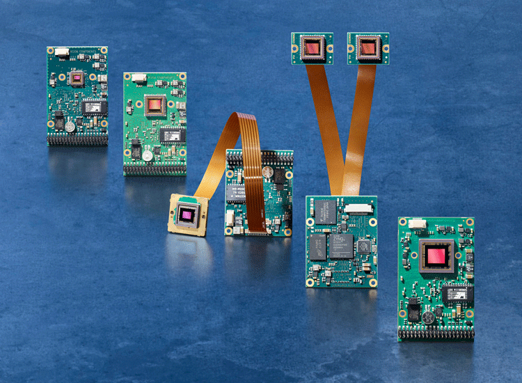
The VCSBC nano Z Series Smart Cameras have been designed for high resolution image processing with a very small form factor. They are the ideal compromise between high performance and low system costs, and thus especially suited for high volume OEM applications. This makes them viable to use a smart camera in even more products than before.
Based on a dual-core processor ARM® Cortex®-A9 with 866 MHz and an integrated FPGA the models of the new VC Z series offer solutions at extreme high-speed in real-time.
The operating system VC Linux provides for the ideal interaction of hard- and software.
All cameras are equipped with a battery backed real time clock and come with 12 programmable input/output signals, with trigger input and flash trigger output, as well as a Gigabit Ethernet interface. Different CMOS sensors (the image resolution can be changed to the ROI required) with global shutter are available.
Some VCSBC nano Z Smart Cameras are also available with remote head (nano Z RH Series).
The extremely low power consumption of only 2.4W makes this camera ideally suitable for use in mobile devices.
1.1 Technical Specifications VCSBC nano Z
| Component / Feature | Specification |
|---|---|
| CMOS Sensor |
|
| Active pixels |
|
| Pixel size |
|
| Active sensor size |
|
| High-speed shutter |
|
| Low-speed shutter |
|
| Integration | Global shutter |
| Picture taking | program-controlled or external high speed trigger, jitterfree acquisition
|
| A/D conversion | 118.75 MHz ( VCSBC nano Z ) / 100 MHz ( VCSBC nano Z-RH ) / 10 bit, only the 8 most significant bits used for grey values |
| Input LUT | yes |
| Image Display | Via 1 Gbit Ethernet onto PC |
| Processor | Dual-Core ARM® Cortex®-A9 with 866MHz and integrated FPGA |
| RAM | 512 MB DDR-SDRAM |
| Flash EPROM | 16 GB flash memory (nonvolatile) industrial eMMC, QSPI Flash |
| Process interface | 12 programmable I/Os |
| Additional LVTTL IOs | I2C Clock and Data signals (I2C also used internally for the Real Time Clock), trigger input (opto-decoupled), Flash output (open collector) |
| Ethernet interface | 1 Gbit |
| Serial interface | RS232 |
| Storage Conditions | Temperature: -20 to +60 deg C, Max. humidity: 90%, non condensing. |
| Operating Conditions | Temperature: 0 to +50 deg C, Max. humidity: 80%, non condensing. |
| Power Supply | 12-24V DC, max. 300 mA |
| Power Consumption | Approx. 2.4W |
The following diagram shows the maximum reachable (with the shortest shutter time) framerate according to the number of captured lines for the VCSBC nano Z 0010, the VCSBC nano Z 0011, the VCSBC nano Z 0015, the VCSBC nano Z 0252 and the VCSBC nano Z 0273:
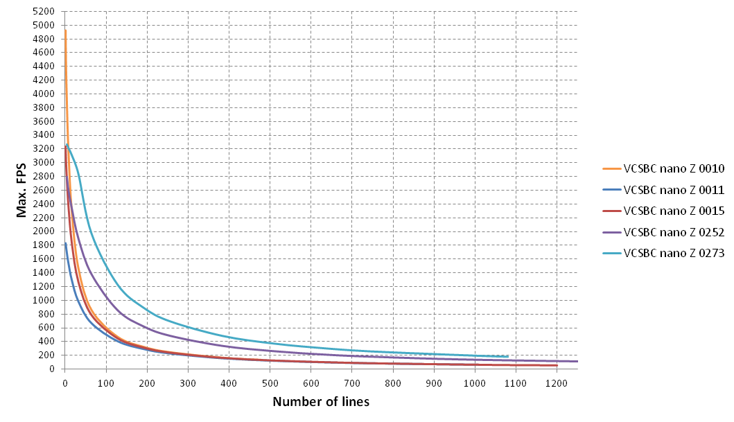
Frames per second over number of lines
The following table gives some example values.
| VCSBC nano Z 0010 | VCSBC nano Z 0011 | VCSBC nano Z 0015 | VCSBC nano Z 0252 | VCSBC nano Z 0273 | |||||
|---|---|---|---|---|---|---|---|---|---|
| Resolution | Max. framerate (FPS) | Resolution | Max. framerate (FPS) | Resolution | Max. framerate (FPS) | Resolution | Max. framerate (FPS) | Resolution | Max. framerate (FPS) |
| 2048 x 1536 | 88 | ||||||||
| 1600 x 1200 | 55 | ||||||||
| 1440 x 1080 | 181 | ||||||||
| 1280 x 1024 | 63 | 1600 x 1024 | 63 | 2048 x 1024 | 134 | 1440 x 1024 | 191 | ||
| 1280 x 768 | 83 | 1600 x 768 | 84 | 2048 x 768 | 177 | 1440 x 768 | 252 | ||
| 1280 x 640 | 98 | 1600 x 640 | 101 | 2048 x 640 | 210 | 1440 x 640 | 300 | ||
| 736 x 480 | 134 | 1280 x 512 | 121 | 1600 x 512 | 125 | 2048 x 512 | 260 | 1440 x 512 | 370 |
| 736 x 384 | 167 | 1280 x 384 | 158 | 1600 x 384 | 164 | 2048 x 384 | 338 | 1440 x 384 | 483 |
| 736 x 256 | 246 | 1280 x 256 | 228 | 1600 x 256 | 240 | 2048 x 256 | 485 | 1440 x 256 | 695 |
| 736 x 192 | 323 | 1280 x 192 | 292 | 1600 x 192 | 312 | 2048 x 192 | 619 | 1440 x 192 | 890 |
| 736 x 128 | 470 | 1280 x 128 | 406 | 1600 x 128 | 447 | 2048 x 128 | 856 | 1440 x 128 | 1227 |
| 736 x 64 | 861 | 1280 x 64 | 669 | 1600 x 64 | 788 | 2048 x 64 | 1382 | 1440 x 64 | 1974 |
| 736 x 32 | 1473 | 1280 x 32 | 986 | 1600 x 32 | 1272 | 2048 x 32 | 1903 | 1440 x 32 | 2843 |
| 736 x 16 | 2288 | 1280 x 16 | 1295 | 1600 x 16 | 1836 | 2048 x 16 | 2340 | 1440 x 16 | 3112 |
| 736 x 8 | 3158 | 1280 x 8 | 1535 | 1600 x 8 | 2359 | 2048 x 8 | 2598 | 1440 x 8 | 3215 |
| 736 x 4 | 3901 | 1280 x 4 | 1691 | 1600 x 4 | 2765 | 2048 x 4 | 2797 | 1440 x 4 | 3267 |
| 736 x 2 | 4422 | 1280 x 2 | 1783 | 1600 x 2 | 3015 | 2048 x 2 | N/A | 1440 x 2 | N/A |
| 736 x 1 | 4925 | 1280 x 1 | 1832 | 1600 x 1 | 3238 | 2048 x 1 | N/A | 1440 x 1 | N/A |
Note
- The measurements were done without any other CPU load. Parallel image processing tasks may lead to a lower framerate.
- These values are only reachable by limiting the maximum image acquisition size at capture initialisation, as explained on this page: Image Acquisition (scroll down to "Changing the Sensor ROI").
- This table is only valid for the VCSBC nano Z camera. The VCSBC nano Z-RH camera has a lower A/D converter frequency and reaches lower framerates.
1.2 Cooling
Cooling using a heat spreader is required. Thermal conductive pads are available as acessoires.
2 Camera Interfaces
2.1 Interface Listings
The pin assignments, electrical specifications as well as available accessories are shown for each interface connector in the following sections.
2.1.1 VCSBC nano Z
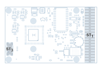
VCSBC nano Z Interfaces
The VCSBC nano Z Series camera boards incorporate the following connector interfaces:
- ST 1
- Power, IO, Ethernet, trigger, serial interface connector
- ST 3
- Emulator Connector
2.1.2 VCSBC nano Z-RH

VCSBC nano Z-RH Interfaces
The VCSBC nano Z-RH Series camera boards incorporate the following connector interfaces:
- ST 1
- Power, IO, Ethernet, trigger, serial interface connector
- ST 3
- Emulator Connector
- ST 4
- Sensor head connector
- ST 5
- Sensor head connector
2.2 ST 1: Power Supply, IO Interface, Ethernet, trigger, serial interface
2.2.1 Pin Assignments ST 1 camera socket
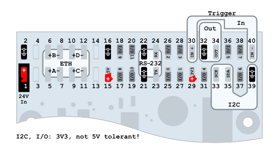
| Signal | Pin | Number | Signal |
|---|---|---|---|
| Power (24V) | 1 | 2 | GND |
| — | 3 | 4 | — |
| Eth A+ | 5 | 6 | Eth B+ |
| Eth A- | 7 | 8 | Eth B- |
| Eth C+ | 9 | 10 | Eth D+ |
| Eth C- | 11 | 12 | Eth D- |
| — | 13 | 14 | — |
| 5V out | 15 | 16 | GND |
| IO_8 | 17 | 18 | IO_9 |
| IO_10 | 19 | 20 | IO_11 |
| GND | 21 | 22 | GND |
| RS232_TX | 23 | 24 | RS232_RX |
| IO_0 | 25 | 26 | IO_2 |
| IO_1 | 27 | 28 | IO_3 |
| 3.3V out | 29 | 30 | Trig_in + |
| IO_4 | 31 | 32 | GND |
| I2C_clock | 33 | 34 | Trig_out |
| I2C_data | 35 | 36 | IO_5 |
| IO_6 | 37 | 38 | IO_7 |
| GND | 39 | 40 | Trig_in - |
2.2.2 Electrical specifications of the VCSBC nano Z Series Power Supply interface
| Nominal Voltage | 12 – 24 V |
| Nominal Power Consumption [1] | 2.4W |
| Minimum operational voltage (including ripple) | 9V |
| Minimum nominal Operating voltage and corresponding current | 12V, 184 mA [2] [3] |
| Maximum nominal Operating voltage and corresponding current | 24V, 99 mA [2] |
| Maximum operational Voltage (including ripple) | 30V |
| 3.3V output maximum current | 100 mA |
| 5V output maximum current | 100 mA |
Power must be connected to pin 1&2 of the ST 1 connector.
Camera power is regulated, so only an unregulated power source of 12 V to 24V is required. The camera is, however, very sensitive to power supply interruption. Please make sure, that the voltage never exceeds the limits of < 9V, > 30V even for a short period of time. In case of trouble it is recommended to back up the power supply by a capacitor or a battery large enough to prevent power interruptions.
The camera may need more current for a short time at startup.
| [1] | Typical power consumption without using the onboard 3.3V supply. |
| [2] | (1, 2) Current drawn from the 3.3V on board signal needs to be added to these figures. |
| [3] | Power consumption may change with processing load and FPGA revision. |
2.2.3 Electrical specifications GPIOs and I2C interfaces
Note
GPIO signals are LVCMOS 3.3V.
| IO_0 – IO_11 | Digital LVCMOS (3.3V) programmable general purpose input / outputs |
| I2C_Clock and I2C_Data | Open collector 3.3V I2C serial Bus Interface for additional peripherals |
| RS232_TX and RS232_RX | Native RS232 serial interface |
The following Signals have a 4k7 pull up resistor on board: - I2C_Clock - I2C_Data
Warning
The I/Os are very sensitive (also to ESD) and not
galvanically separated. Opto-isolation of the driving circuit is
therefore strongly recommended. It is also recommended to keep the cable
as short as possible!
Please note that the I/Os are not protected against over current. The I/Os are neither protected against short circuit nor reverse voltage spikes from inductive loads.
Note
Use the VC nano Z Series or the VC pro Z Series
cameras if you cannot provide a suitable I/O driving circuit. These
cameras include the same hardware as the VCSBC nano Z Series Smart
Cameras, but overcurrent protection of the inputs and outputs is already
included.
2.2.4 Electrical specifications trigger input and output
Note
Activation of trigger output is done by assigning the right GPIO via the command line tool named vcio, see GPIOs and Trigger Assignment for more information.
2.2.4.1 Trigger IO Specifications
The board features a dedicated fast trigger input (opto-isolated, for use as image capture trigger) and a fast trigger output (as strobe-light trigger). Since both signals are fast at a very low noise margin, it is recommended to keep the cable as short as possible. Use twisted pair or even coaxial cable for this purpose. The trigger input assures a constant image capture delay without jitter.
2.2.4.2 Circuit trigger input and output
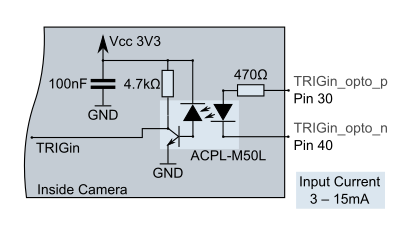
Circuit at Trigger Inputs
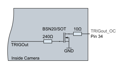
Circuit at Trigger Outputs
2.2.4.3 Example of driving circuit for the trigger input and output
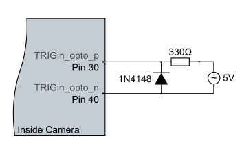
Connection of Trigger Inputs
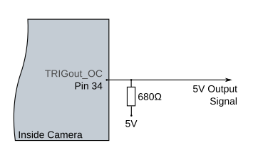
Connection of Trigger Outputs
2.2.5 Realtime clock and backup battery
The board contains a realtime clock (RTC) with battery backup. The RTC is set during manufacturing to the current date and time. For backup a rechargeable lithium coin cell battery is used. This battery is charged to only about 10 percent of the nominal capacity on delivery and may be empty after a prolonged period of storage. We recommend charging the battery for at least 50 hours and setting the RTC (linux command: hwclock and date) when the board is first used (battery charges automatically when the system is powered on). The battery contains so little lithium, that it is not listed as a hazardous device for the environment and the flight export regulations. For details please refer to https:// industrial.panasonic.com/ww/products/batteries/secondary-batteries/ coin_rechargeable_lithium/coin-type-rechargeable-lithium-batteries-ml- series/ML621
| Battery Manufacturer | Panasonic |
|---|---|
| Battery Type | ML621 |
| Nominal Voltage | 3V |
| Nominal Capacity | 5 mAh |
| Charging Time for 100% Capacity | 100h |
| Charging Time for 80% Capacity | 50h |
| Backup Retention Time for 100% Charged Battery | 200 days |
Note
To check if the hardware clock is set appropriately, scan the output of the following linux shell command:
dmesg | grep rtc
One response line may contain the following message:
[ 0.322074] rtc-ds1374 0-0068: oscillator discontinuity flagged, time unreliable
This indicates low battery status or battery discontinuity.
To set the hardware clock it is necessary to set the software clock first:
date -s "2017-11-21 11:47:00"
Then the software clock time is transferred to the realtime clock by the following command:
hwclock -w
3 Software Interfaces
3.1 GPIOs
| GPIO Nr. | Pin Designator | Usability | Remark |
|---|---|---|---|
| 0 | IO 0 | Input/Output | Input Undebounced |
| 1 | IO 1 | Input/Output | Input Undebounced |
| 2 | IO 2 | Input/Output | Input Undebounced |
| 3 | IO 3 | Input/Output | Input Undebounced |
| 4 | IO 4 | Input/Output | Input Undebounced |
| 5 | IO 5 | Input/Output | Input Undebounced |
| 6 | IO 6 | Input/Output | Input Undebounced |
| 7 | IO 7 | Input/Output | Input Undebounced |
| 8 | IO 8 | Input/Output | Input Undebounced |
| 9 | IO 9 | Input/Output | Input Undebounced |
| 10 | IO 10 | Input/Output | Input Debounced |
| 11 | IO 11 | Input/Output | Input Debounced |
| 12 | — | — | — |
| 13 | — | — | — |
| 14 | — | — | — |
| 15 | — | — | — |
| 16 | — | — | — |
| 17 | — | — | — |
| 18 | — | — | — |
| 19 | — | — | — |
| 20 | — | — | — |
| 21 | — | — | — |
| 22 | — | — | — |
| 23 | — | — | — |
| 24 | — | — | — |
| 25 | — | — | — |
| 26 | — | — | — |
| 27 | — | — | — |
| 28 | — | — | — |
| 29 | — | — | — |
| 30 | — | — | — |
| 31(Out) | TrigOut | Output | — |
| 31(In ) | TrigIn | Input | Optically isolated; debounced only for sensor trigger, not for linux GPIO. |
They can be accessed over the linux standard way via /sys/class/gpio, see https://www.kernel.org/doc/Documentation/gpio/sysfs.txt. The GPIO numbers are relative to the start number of the gpiochip labelled with '/amba@0/axi-gpio0@41200000', here: /sys/class/gpio/gpiochip224.
The debouncing time can be adjusted via the vcio command, using the same timing for all debouncers.
You can also find information in our libvclinux documentation. This documentation can be found in the support area of our website: https://www.vision-components.com/fileadmin/external/documentation/software/lib/libvclinux/latest/html/index.html
3.2 Trigger Assignment
To choose the sensor input/output trigger signals, the corresponding GPIO Nr. must be determined and assigned by the supporting program named vcio. More information can be found at the help of the program, if you run it with no command line parameter, it will show how to do it. Sample usage instructions are provided here, but always refer to the instructions of your version:
VCIO v.1.2.3.- VCLinux Camera I/O Configuration and Connection Setup.
Usage: vcio [-s sen] [-i gpioNr] [-n] [-o gpioField] [-d gpioField] [-t time]
-s Sensor to be configured, default value: 0. -i GPIO Nr. to be used as external sensor trigger input (TRGSRC_EXT) -n Negates trigger input signal -o Bitfield of GPIOs which are coupled with sensor trigger output signal. The bit of GPIO Nr. X is coupled, if Bit X is set to 1, for example, For coupling GPIO Nr. 0, 3 and 31 (TrigOut) provide the Bitfield as Decimal Value: 2^0+2^3+2^31=2147483657, as Hex Value: 0x80000009, or as Binary Value: 0b10000000000000000000000000001001. -d The direction of the GPIOs as bitfield (see -o switch); If the GPIO Nr. X should be configured as output, set bit X to 1, and if it should be an input, set bit X to 0. -t Time used to debounce all input sources, default value: 10000. Time Unit is in FPGA Cycles. The FPGA clock frequency can be acquired by reading out the value of capt->sen->d.fpgaClkHz, e.g. 153846161 Hz. The default debouncing time for that example is then given by 10000 cycles / 153846161 Hz = 0.000065 s = 65 us. Settings done cannot be read out. Different camera models may have different vcio parameters.
Example
If an additional flash device is connected to Pin IO 1,
the 'Connector Assignment of GPIOs' table shows the corresponding GPIO Nr.: 1.
To link the gpio Nr. 1 to the sensor trigger signal, the 'vcio' program must make the gpio Nr. 1 an
output gpio (-d) and couple it to the sensor trigger signal (-o), for example,
the following call uses the TrigOut pin (gpio Nr. 31) and the IO 1 pin
(gpio Nr. 1) for simultaneous flash output, the external input trigger is coming
from gpio Nr. 10, which is, by table, the hardware pin of IO 10:
vcio -d 0b10000000000000000000000000000010 -o 0x80000002 -i 10
One can further switch flash outputs for each capture (see the libvclinux documentation: VCFlashSelector); therefore the corresponding gpios must be set as output (-d), but they should not be coupled with the trigger signal (-o), since this given value would be ORed with the flash selector settings, and the flash would always trigger.
Note
To actually use the trigger input source (assigned by the vcio program) you have to select it at your source code in your image capture struct by setting the capture trigger input source to TRGSRC_EXT (instead of TRGSRC_IMM for immediate trigger); refer to the libvclinux image acquisition documentation! You may also invert the trigger signal first, see Output Trigger Signal Inversion
| GPIO Nr. | Pin Designator | Assignment |
|---|---|---|
| 31(Out) | TrigOut | Trigger Output |
| 31(In ) | TrigIn | Trigger Input |
3.2.1 Output Trigger Signal Inversion
One can invert the value of the trigger output signal by writing a 1 onto the corresponding GPIO nr, for example via the program 'vcgpio'. To get usage instruction for the program vcgpio run it without any parameters. The figure shows how it is applied.
3.2.2 Input-Output Circuit

VC nano Z I/O Circuit
The debouncing time can be adjusted via the vcio command, using the same timing for all debouncers.
4 OEM models with VC nano 3D Z FPGA
Some models are available with the VC nano 3D Z FPGA, for customers wanting to build a custom laser triangulation system using a VC camera and a separate laser.
Note
In this case, the whole GPIO configuration corresponds to the VC nano 3D Z GPIO configuration, see chapter 3 of the VC nano 3D Z documentation:
https://www.vision-components.com/fileadmin/external/documentation/hardware/VC_nano_3D_Z/index.html
A laser can then be connected to OUT3, which can be activated as an additional trigger output. The standard trigger output is limited to a duration of 100 µs, using the alternative trigger output OUT3 allows to overcome this limitation.
5 Accessories
5.1 Camera and Lens holder order numbers
| Order Number | Product / Service description |
|---|---|
| VK002237 | VCSBC nano Z 0010 Smart Camera without lens holder, b/w sensor |
| VK002857 | VCSBC nano Z 0010 Smart Camera without lens holder, color sensor |
| VK002087 | VCSBC nano Z 0011 Smart Camera without lens holder, b/w sensor |
| VK002131 | VCSBC nano Z 0011 Smart Camera without lens holder, color sensor |
| VK002132 | VCSBC nano Z 0015 Smart Camera without lens holder, b/w sensor |
| VK003115 | VCSBC nano Z 0252 Smart Camera without lens holder, b/w sensor |
| VK003310 | VCSBC nano Z 0273 Smart Camera without lens holder, b/w sensor |
| VK003150 | VCSBC nano Z 0392 Smart Camera without lens holder, b/w sensor |
| VK002267 | VCSBC nano Z-RH 0010 Smart Camera without lens holder, b/w sensor |
| VK002115 | VCSBC nano Z-RH 0011 Smart Camera without lens holder, b/w sensor |
| VK002184 | VCSBC nano Z-RH 0011 Smart Camera without lens holder, color sensor |
| VK002124 | VCSBC nano Z-RH 0012 Smart Camera without lens holder, b/w sensor |
| VK002881 | VCSBC nano Z-RH 0252 Smart Camera without lens holder, b/w sensor |
| VK003110 | VCSBC nano Z-RH 0252 Smart Camera without lens holder, color sensor |
| VK003108 | VCSBC nano Z-RH 0273 Smart Camera without lens holder, b/w sensor |
| VK003169 | VCSBC nano Z-RH 0273 Smart Camera without lens holder, color sensor |
| VK002116 | VCSBC nano Z-RH-2 0011 Smart Camera without lens holder, b/w sensor |
| VK002129 | VCSBC nano Z-RH-2 0011 Smart Camera without lens holder, color sensor |
| VK002192 | VCSBC nano Z-RH-2 0015 Smart Camera without lens holder, color sensor |
| VK003319 | VCSBC nano Z 0252 Smart Camera without lens holder, b/w sensor, with VC nano 3D Z FPGA |
| VK000439 | VCSBC nano Z-RH 0252 Smart Camera without lens holder, b/w sensor, with VC nano 3D Z FPGA |
| VK000442 | VCSBC nano Z-RH 0273 Smart Camera without lens holder, b/w sensor, with VC nano 3D Z FPGA |
| VK002092 | Lens holder C Mount |
| VK000091 | Lens holder 12mm |
| EK001348 | Thermal Pad 23mm x 23mm x 2mm, 5.5 W/(m * K) |
Further models will be offered.
5.2 Further accessories available for VCSBC nano Z Smart Cameras
| Article Description | Order Number |
|---|---|
| Power adapter for rail mounting, Input Voltage 100 – 240VAC 50/60 Hz Output Voltage DC 24V +/-5%, max. 300 mA (7.5 W) Equipped with connecting clamps for AC input and 24V output, CE cert. | VK000036 |
| Evaluation cable (for testing), 24-pin, with RJ45 connector (Ethernet), DB9 connector (RS232) and banana plugs for power supply | VK002079 |
| Thermal conductive pad 40x40x2mm | EK001122 |
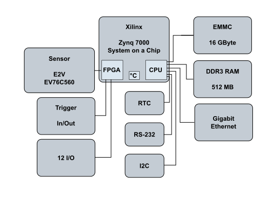
6 Appendix A: Block diagram VCSBC nano Z Series
The image is formed by a 1.3 megapixel CMOS sensor (VCSBC nano Z 0011). The image is then stored in the DDR3-SDRAM memory, which has been increased to 512 MB.
Block diagram |VCSBC_nano_Z| Series
7 Appendix B: Drawing Circuit Board VCSBC nano Z Series
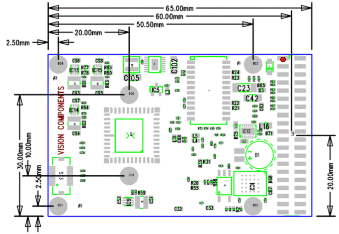
The red dot  marks the Pin 1 position of each connector.
Tolerances: All circuit board dimensions: +/- 0.1mm
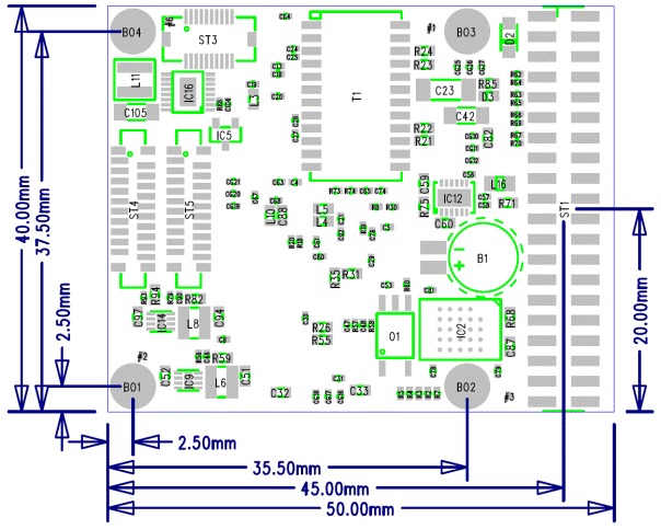
8 Appendix C: Drawing Circuit Board VCSBC nano Z-RH Series
Camera Board
Sensor Board (for RH camera models 0010, 0011, 0012)
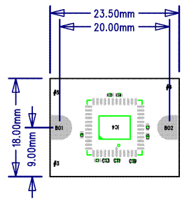
The red dot  marks the Pin 1 position of each connector.