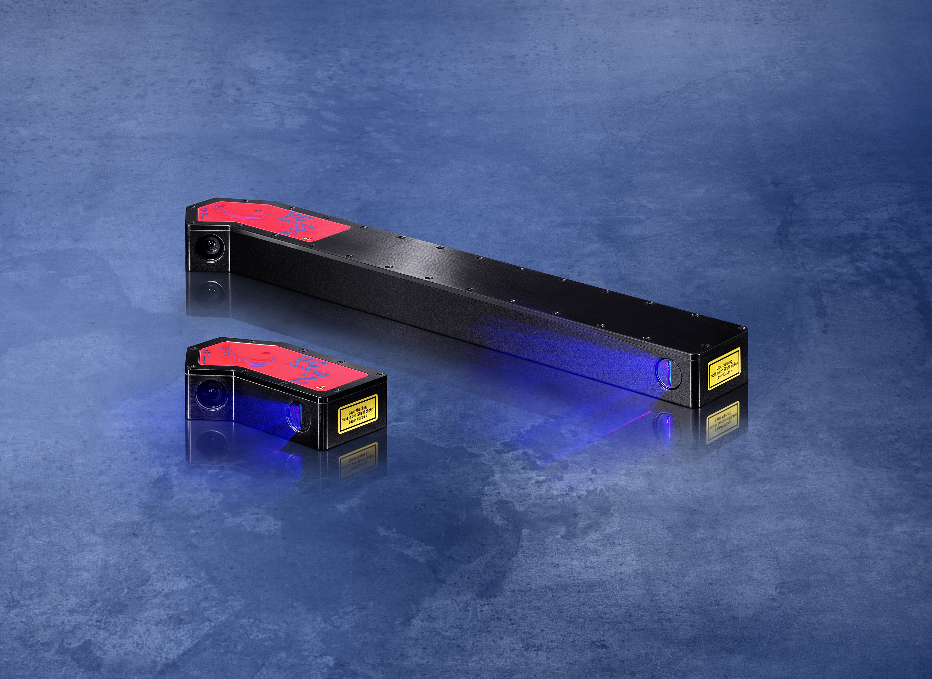
VC nano 3D-Z Series Operating Manual
Hardware specifications of VC nano 3D-Z Laser Profilers
| Revision: | 1.3.1 |
|---|---|
| Date: | 2023-03-01 |
| Contact: | support@vision-comp.com |
| Copyright: | 1996-2023 Vision Components GmbH Ettlingen, Germany |
| Author: | VC Support, mailto:support@vision-comp.com |
This documentation has been prepared with most possible care. However Vision Components GmbH does not take any liability for possible errors. In the interest of progress, Vision Components GmbH reserves the right to perform technical changes without further notice.
Please notify support@vision-components.com if you become aware of any errors in this manual or if a certain topic requires more detailed documentation.
This manual is intended for information of Vision Component’s customers only. Any publication of this document or parts thereof requires written permission by Vision Components GmbH.
| Symbol | Meaning |
|---|---|
 |
The Light bulb highlights hints and ideas that may be helpful for a development. |
 |
This warning sign alerts of possible pitfalls to avoid. Please pay careful attention to sections marked with this sign. |
 |
This is a sign for an example. |
Trademarks
Linux, Debian, the Tux logo, Vivado, Xilinx and Zynq, ARM, Cortex, Windows XP, Total Commander, Tera Term, Motorola, HALCON, FreeRTOS, Vision Components are registered Trademarks. All trademarks are the property of their respective owners.
Table of Contents
1 General Information
| Component / Feature | Specification |
|---|---|
| Laser | Class 2, <100mW average, wave length 450nm |
| CMOS Sensor | 1/2.9" sony IMX273LLR, monochrome version |
| Active pixels | 1408(H) x 1080(V) |
| Pixel size | 3.45(H) x 3.45(V) µm |
| Active sensor size | 4.8(H) x 3.7(V) mm |
| High-speed shutter | 1 µsec + steps of 1 µsec |
| Integration | Global shutter |
| Data acquisition | program-controlled or external high speed trigger, jitter-free acquisition full-frame up to 174 frames per second |
| A/D conversion | 10 bit, 8 bits used after LUT application |
| Input LUT | 1024 x 8 bits |
| Image Display | Via Ethernet onto PC |
| Processor | Dual-Core ARM® Cortex®-A9 with 866MHz and integrated FPGA |
| FPGA | Laser line processing during image acquisition in FPGA |
| RAM | 512 MB DDR-SDRAM |
| Flash EPROM | 16 GB flash memory (nonvolatile) industrial eMMC |
| Process interface | See following description. |
| Encoder Inputs | Yes, and encoder inputs can be used as additional 5-24V inputs. |
| Trigger Input | Encoder Signal A can be used as trigger input. |
| Ethernet interface | 1 Gbit / 100 Mbit / 10 Mbit |
| CE certification | CE Certification from Vision Components |
| Storage Conditions | Temperature -20 to +60 deg C, Max. humidity: 90%, non condensing. |
| Operating Conditions | Temperature: 0 to +50 deg C, Max. humidity: 80%, non condensing. |
| Power Supply | 24V DC, 300mA without I/O usage. |
| Power Consumption | 7.2 W typical without I/O usage. |
1.1 Technical Specification VC nano 3D-Z
1.1.1 Framerate calculation
the framerate can be calculated by following these subcalculations:
- Calculate the time for a video line: TLine = HMAX*13.468 ns.
- Calculate the time for storing the captured image: TCapt = (DY + 33 + FPGADelay)*TLine + 3.3us.
- Calculate the total time: TTotal = ShutterTime + TCapt.
FPGADelay in NrOfProcessingLines, between 7 and 38, depending on the filter configuration; main impact has the bgSubKy setting (see the libvclinux documentation).
| DX | HMAX | TLine (us) |
|---|---|---|
| 1408 | 370 | 4.983 |
| 1344 | 350 | 4.713 |
| 1280 | 330 | 4.444 |
| 1216 | 320 | 4.310 |
| 1152 | 300 | 4.040 |
| 1088 | 290 | 3.906 |
| 1024 | 270 | 3.636 |
| 960 | 250 | 3.367 |
| 896 | 240 | 3.232 |
| 640 | 240 | 3.232 |
| 320 | 240 | 3.232 |
The following tables show some examples.
| DY/DX | 1408 | 1344 | 1280 | 1216 | 1152 | 1088 | 1024 | 960 | 896 | 640 | 320 |
|---|---|---|---|---|---|---|---|---|---|---|---|
| 1080 | 5.584 | 5.283 | 4.981 | 4.830 | 4.529 | 4.378 | 4.076 | 3.774 | 3.623 | 3.623 | 3.623 |
| 1024 | 5.305 | 5.019 | 4.732 | 4.589 | 4.302 | 4.159 | 3.872 | 3.586 | 3.442 | 3.442 | 3.442 |
| 960 | 4.986 | 4.717 | 4.448 | 4.313 | 4.044 | 3.909 | 3.640 | 3.370 | 3.236 | 3.236 | 3.236 |
| 800 | 4.189 | 3.963 | 3.737 | 3.623 | 3.397 | 3.284 | 3.058 | 2.832 | 2.718 | 2.718 | 2.718 |
| 512 | 2.754 | 2.605 | 2.457 | 2.382 | 2.234 | 2.159 | 2.011 | 1.862 | 1.788 | 1.788 | 1.788 |
| 256 | 1.478 | 1.399 | 1.319 | 1.279 | 1.199 | 1.159 | 1.080 | 1.000 | 0.960 | 0.960 | 0.960 |
| 128 | 0.840 | 0.795 | 0.750 | 0.727 | 0.682 | 0.659 | 0.614 | 0.569 | 0.546 | 0.546 | 0.546 |
| DY/DX | 1408 | 1344 | 1280 | 1216 | 1152 | 1088 | 1024 | 960 | 896 | 640 | 320 |
|---|---|---|---|---|---|---|---|---|---|---|---|
| 1080 | 5.739 | 5.429 | 5.119 | 4.964 | 4.654 | 4.499 | 4.189 | 3.879 | 3.724 | 3.724 | 3.724 |
| 1024 | 5.460 | 5.165 | 4.870 | 4.722 | 4.428 | 4.280 | 3.985 | 3.690 | 3.543 | 3.543 | 3.543 |
| 960 | 5.141 | 4.863 | 4.586 | 4.447 | 4.169 | 4.030 | 3.752 | 3.475 | 3.336 | 3.336 | 3.336 |
| 800 | 4.344 | 4.109 | 3.874 | 3.757 | 3.522 | 3.405 | 3.171 | 2.936 | 2.819 | 2.819 | 2.819 |
| 512 | 2.908 | 2.751 | 2.594 | 2.516 | 2.359 | 2.280 | 2.123 | 1.966 | 1.888 | 1.888 | 1.888 |
| 256 | 1.633 | 1.545 | 1.457 | 1.413 | 1.325 | 1.280 | 1.192 | 1.104 | 1.060 | 1.060 | 1.060 |
| 128 | 0.995 | 0.941 | 0.888 | 0.861 | 0.807 | 0.781 | 0.727 | 0.673 | 0.647 | 0.647 | 0.647 |
| DY/DX | 1408 | 1344 | 1280 | 1216 | 1152 | 1088 | 1024 | 960 | 896 | 640 | 320 |
|---|---|---|---|---|---|---|---|---|---|---|---|
| 1080 | 179 | 189 | 201 | 207 | 221 | 228 | 245 | 265 | 276 | 276 | 276 |
| 1024 | 188 | 199 | 211 | 218 | 232 | 240 | 258 | 279 | 290 | 290 | 290 |
| 960 | 201 | 212 | 225 | 232 | 247 | 256 | 275 | 297 | 309 | 309 | 309 |
| 800 | 239 | 252 | 268 | 276 | 294 | 304 | 327 | 353 | 368 | 368 | 368 |
| 512 | 363 | 384 | 407 | 420 | 448 | 463 | 497 | 537 | 559 | 559 | 559 |
| 256 | 676 | 715 | 758 | 782 | 834 | 863 | 926 | 1000 | 1042 | 1042 | 1042 |
| 128 | 1190 | 1258 | 1333 | 1375 | 1466 | 1516 | 1628 | 1758 | 1830 | 1830 | 1830 |
| DY/DX | 1408 | 1344 | 1280 | 1216 | 1152 | 1088 | 1024 | 960 | 896 | 640 | 320 |
|---|---|---|---|---|---|---|---|---|---|---|---|
| 1080 | 174 | 184 | 195 | 201 | 215 | 222 | 239 | 258 | 269 | 269 | 269 |
| 1024 | 183 | 194 | 205 | 212 | 226 | 234 | 251 | 271 | 282 | 282 | 282 |
| 960 | 195 | 206 | 218 | 225 | 240 | 248 | 266 | 288 | 300 | 300 | 300 |
| 800 | 230 | 243 | 258 | 266 | 284 | 294 | 315 | 341 | 355 | 355 | 355 |
| 512 | 344 | 363 | 385 | 397 | 424 | 439 | 471 | 509 | 530 | 530 | 530 |
| 256 | 612 | 647 | 687 | 708 | 755 | 781 | 839 | 906 | 943 | 943 | 943 |
| 128 | 1005 | 1062 | 1126 | 1162 | 1239 | 1281 | 1376 | 1485 | 1547 | 1547 | 1547 |
Note
- The measurements were done without any other CPU load. Parallel image processing tasks may lead to a lower framerate.
- These values are only reachable if image capturing is deactivated.
1.1.2 Measurement specifications
VC offers a wide range of models of VC nano 3D-Z sensors concerning field of view and resolution. The following table shows some examples. For additional models see the links below. Please contact us for custom designs.
| Model (focal distance [mm] / angle [deg]) | (8/30) regular | (8/34) regular | (8/30) large | (8/34) large | (8/30) xlarge | (8/34) xlarge | (8/30) xxlarge | (8/34) xxlarge | (6/32) regular |
|---|---|---|---|---|---|---|---|---|---|
| Minimal distance Z [mm] | 90 | 80 | 170 | 150 | 285 | 245 | 460 | 400 | 70 |
| Maximal distance Z [mm] | 245 | 195 | 470 | 375 | 785 | 625 | 1285 | 1020 | 285 |
| Min. horizontal field of view X [mm] | 65 | 65 | 130 | 120 | 215 | 200 | 350 | 325 | 80 |
| Max. horizontal field of view X [mm] | 150 | 125 | 295 | 240 | 495 | 400 | 810 | 660 | 230 |
| Resolution X Min [µm] | 60 | 50 | 110 | 100 | 170 | 160 | 280 | 260 | 70 |
| Resolution X Max [µm] | 120 | 100 | 240 | 190 | 390 | 320 | 640 | 520 | 190 |
| Resolution Z Min [µm] | 10 | 10 | 20 | 20 | 30 | 30 | 40 | 40 | 10 |
| Resolution Z Max [µm] | 40 | 30 | 80 | 60 | 130 | 90 | 220 | 150 | 70 |
A more comprehensive list of possible models:
2 Hardware Interfaces

Connector Positions
The VC nano 3D-Z camera incorporates the following connector interfaces:
| Connector | Description |
|---|---|
| J0 | Power Connector |
| JE | Ethernet Connector |
A detailled description of the connectors follows below.
2.1 Power Connector J0
2.1.1 J0 Pin Assignment
| Camera Socket Rear View | Pin | Signal | Level | Cable Standard Color |
|---|---|---|---|---|
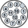 |
1 | Main Power Supply | +24 V | brown |
| 2 | Common Ground | GND | blue | |
| 3 | INP 0 or Laser Enable | +5–24 V | white | |
| 4 | OUT 0 | +24 V | green | |
| 5 | INP 1 or ENC Z or Trigger Enable | +5–24 V | pink | |
| 6 | OUT 1 | +24 V | yellow | |
| 7 | OUT 2 | +24 V | black | |
| 8 | INP 2 or ENC A or TrigIn | +5–24 V | grey | |
| 9 | OUT 3 or TrigOut [1] | +24 V | red | |
| 10 | INP 3 or ENC /B | +5–24 V | purple | |
| 11 | INP 4 or ENC B | +5–24 V | grey/pink | |
| 12 | INP 5 or ENC /A | +5–24 V | red/blue |
| [1] | TrigOut only supported at custom OEM versions. |
All outputs are high-side switches, 24V, 400mA max.
All inputs and encoder inputs are 5-24V, 3mA, 200kHz max.
| Signal | Description |
|---|---|
| INP 0 – INP 5 | PLC inputs. |
| OUT 0 – OUT 3 | PLC outputs. |
| Laser Enable | Hardware safety signal for the activation of the laser, must be set to high to enable the laser. It completely shuts down the power supply of the laser. Feature depending on hardware option. Does not influence triggering. |
| TrigIn | External trigger for image capture. |
| Trigger Enable | External signal to activate capturing, must be set to high for the complete capturing process. If signal is set to low, triggers will be blocked. |
| ENC A, ENC /A, ENC B, ENC /B, ENC Z | Encoder signals. |
| TrigOut | External trigger output, only supported at OEM custom versions; Other versions will be inaccurate! |

Trigger Schematics
If the Laser Warden is used and no Laser Enable is given, the capture will be done nevertheless but without active laser.

Laser Power Supply Control Schematics
2.1.2 Electrical Specification: Camera Power Supply
| What | How much |
|---|---|
| Nominal Voltage | +24 V |
| Absolute Maximum Voltage Limit | +32V |
| Minimum recommended Operating voltage | 21.6V |
| Maximum recommended Operating voltage | 26.4V |
| Operating Current (Typical) | 260mA |
| Operating Current (Maximum) | 300mA |
| Nominal Power Consumption (Typical) | 6.5W |
| Nominal Power Consumption (Maximum) | 7.2W |
2.1.3 Electrical Specification: Digital PLC I/O, Encoder
| Separation of PLC/trigger output voltage | PLC outputs supply not separated from power supply |
| PLC Input Voltage | +5–24 V |
| Input Current (max) | 3mA, Threshold: Positive: +1.3mA typ., Negative: 0.7mA typ. |
| PLC Output Voltage | 24V |
| PLC Output Current (max) | 4 x 400 mA Max total of all outputs: 1A |
| Max Current for 1 Power / PLC connector pin | 400 mA |
| Loads | Resistive, inductive and capacitive possible |
| Output Protection | Yes: short circuit, overcurrent, temperature |
| Power failure detection | Yes, power failure detected if total PLC current > 1A |
Warning
If power failure is detected, all PLC outputs may switch off
regardless of their output state for hardware protection.
2.1.3.1 Connection of PLC, Encoder inputs VC nano 3D-Z Series
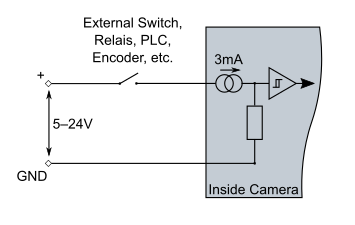
Connection of PLC Inputs
2.1.3.2 Connection of PLC outputs VC nano 3D-Z Series
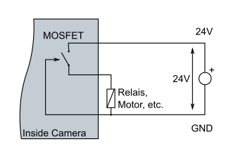
Connection of PLC Outputs
2.1.4 Encoder input specification VC nano 3D-Z Series
It is possible to connect the following encoder signals: ENC A, ENC /A, ENC B, ENC /B, ENC Z. There is no connection provided for signal ENC /Z.
Timings for Encoder Pins
| ENC A | ENC /A | ENC B | ENC /B | ENC Z | Remarks |
|---|---|---|---|---|---|
| X | — | — | — | — | Not recommended |
| X | X | — | — | — | |
| X | — | X | — | — | Only recommended for cables < 5m |
| X | — | X | — | X | Only recommended for cables < 5m |
| X | X | X | X | — | Most noise tolerant |
| X | X | X | X | X | Most noise tolerant |
Due to noise and signal bouncing the configuration using only ENC A signal is not recommended.
Pins not used for the encoder can be used as GPIO inputs.
It is possible to swap the signals A and B per software.
The maximum encoder frequency is limited to 200 kHz.
Warning
If the ENC Z signal is used, but the full-step resolution of the encoder
is not programmed correctly, triggering may stop working after some
occurences.
2.1.4.1 Encoder Counter

Encoder Counter
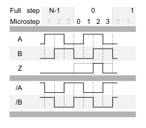
All internal encoder values represent positions with microstep resolution: A counter is used internally for counting the full-steps (Bits 31 to 2), whereas the microsteps (Bits 2 to 0) are directly derived from the encoder signals ENC A and ENC B.
The ENC Z signal is detected during microsteps 1 and 2. It resets the full-step counter without resetting the value of the microstep: I.e. the output value during reset can be 0, 1, 2 or 3 depending on the microstep position of the encoder.
If the ENC Z signal is used, the user must program the full-step resolution of the encoder for correct operation, else triggers may not work anymore after some cycles. This number is usually documented at the data sheet of the encoder device. The encoder counts even before the first ENC Z signal is detected. Until then the encoder counter value may be considered as invalid. It is a common practice to calibrate the encoder, moving it to a zero position (reference) first. For your convenience the GPIO input signal 28 is provided indicating that a first ENC Z impulse has been detected. Loss of calibration is indicated if the GPIO input signal 27 is set. This may happen if the ENC Z signal is inconsistent with the full-step resolution. This may occur due to noise, broken cable or a wrong setting for the encoder full-step resolution.
The encoder position at the image trigger is stored in memory for possible later reference.
Note
In case of doubt, the correct programming of the encoder's full-step resolution is verifyable over the GPIO signal 27.
2.1.4.2 Encoder Trigger
Scanline Triggering for K = 5
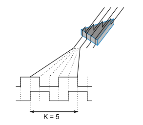
This internal hardware module allows for the generation of triggers every K microsteps (see figure). It allows to control the spacing of the scanlines with high resolution.
At very low encoder speed the encoder position may occasionally move slightly backwards. In this case there will be no trigger until the encoder reaches the next valid trigger position in forward direction.
Although the encoder trigger is internal, for the image acquisition it acts as like an 'external trigger'. Triggers may be lost during the image acquisition time.
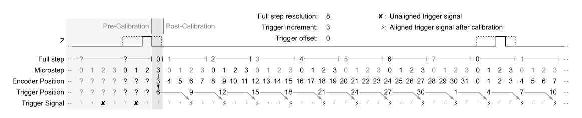
At startup time the system is in an uncalibrated state. This state can also be re-entered when the program 'vcio' is called without the option '-R'. When the first ENC Z signal in positive direction occurs, the system is calibrated, i.e. the encoder position is set to zero plus the current microstep and the next trigger position is set as follows:
trigger position = microstep + trigger increment + trigger offset.
The re-entering done at 'vcio' is a pseudo-calibration like using the Z signal at this encoder position which is all that is necessary for systems without an ENC Z signal.
If the ENC Z signalling is active, each incoming ENC Z signal resets the encoder position counter to zero plus the current microstep, in contrast to the trigger position which is only reset at calibration time.
Example for encoder/trigger acting
Example
Given the encoder full-step resolution is 8 and the trigger increment 3.
and the last trigger position of the first revolution is 30. The encoder counter then counts to encoder position 31 and wraps around to 0.
The following trigger signals then occur at positions: 1, 4, 7, …
Note
If increment plus offset is greater than or equals the full-step resolution times 4 trigger signals may never occur.
The encoder does not require an ENC Z signal. Such a system is called an uncalibrated system. It produces the trigger signals relative to a virtual zero which was set at the start of the system and can be set manually by calling 'vcio'. For systems using the ENC Z signal the situation is similar up to the point where the ENC Z signal occurs. I.e. there may be a number of uncalibrated trigger impulses before the occurrence of the ENC Z signal. After the occurrence of the ENC Z signal the system is calibrated, i.e. the trigger impulses are relative to the absolute zero set by the ENC Z signal at calibration time. The GPIO input signal 28 is provided indicating that a first ENC Z impulse has been detected.
Note
Always check the direction of the encoder movement if no or not enough trigger impulses occur.
You can change the interpretation of the direction via the 'vcio' program.
Warning
During image acquisition, additional triggers may be lost.
2.2 Ethernet Connector JE
2.2.1 JE Pin Assignment
| Camera Socket Rear View | Pin | Signal |
|---|---|---|
 |
1 | ETH_A_p |
| 2 | ETH_A_n | |
| 3 | ETH_B_p | |
| 4 | ETH_B_n | |
| 5 | ETH_D_p | |
| 6 | ETH_D_n | |
| 7 | ETH_C_n | |
| 8 | ETH_C_p |
2.3 Electrical Specification: Laser
| Laser class | 2 |
| Power | <100mW |
| Wave lenght | 450nm |
| Maximum pulse duration | 100us |
| Maximum duty cycle | 1:7 |
If the acquisition time exceeds the maximum pulse duration of the laser, the laser will be switched off.
The duty cycle is limited to 1:7, i.e. the off-state is six times longer than the on-state for the laser output.
Example
100 us pulse duration, 600 us cool down duration.
2.4 Status LEDs
The VC nano 3D-Z Laser Profilers feature 4 LEDs providing status information as listed at the following table.
| Status LED | Meaning if light is turned on |
|---|---|
| POW: Power ON | The camera system is powered. |
| ON: Laser ON | The laser emits light. |
| OVL: Laser Overload | The laser does not emit light due to excess of the maximum allowed acquisiton time. |
| EN: Laser Permission | The laser does not emit light due to missing permission. |
| STA: Trigger | Toggles on/off for each internal encoder trigger. |
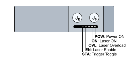
Status LED Positions
3 Software Interfaces
3.1 GPIOs
| GPIO Nr. | Connector | Pin Designator | Usability | Remark |
|---|---|---|---|---|
| 0 | J0 | OUT 0 | Output | — |
| 1 | J0 | OUT 1 | Output | — |
| 2 | J0 | OUT 2 | Output | — |
| 3 | J0 | OUT 3 | Output | In case OUT 3 is configured as TrigOut, this GPIO inverts the polarity of the signal if set. |
| 4 | INTERNAL | Laser enable | Output | Activates laser power supply if set to 1, active only if external Laser Warden laser enable is not active. |
| 5 | — | — | — | — |
| 6 | — | — | — | — |
| 7 | — | — | — | — |
| 8 | — | — | — | — |
| 9 | — | — | — | — |
| 10 | J0 | INP 0 | Input | — |
| 11 | J0 | INP 1 | Input | — |
| 12 | J0 | INP 2 | Input | — |
| 13 | J0 | INP 3 | Input | — |
| 14 | J0 | INP 4 | Input | — |
| 15 | J0 | INP 5 | Input | — |
| 16 | — | — | — | — |
| 17 | — | — | — | — |
| 18 | — | — | — | — |
| 19 | — | — | — | — |
| 20 | — | — | — | — |
| 21 | — | — | — | — |
| 22 | — | — | — | — |
| 23 | — | — | — | — |
| 24 | — | — | — | — |
| 25 | — | — | — | — |
| 26 | — | — | — | — |
| 27 | INTERNAL | Counter mismatch detector | Input | Set to 1 if ENC Z impulse detected while internal counter not 0, requires encoder counter reset to be cleared. Nevertheless the counter will be reset to zero. |
| 28 | INTERNAL | Encoder calibration done | Input | Set to 1 after first ENC Z impulse detected. Used to indicate the validity of the encoder counter values. |
| 29 | INTERNAL | MALFUNCTION | Input | — |
| 30 | — | — | — | — |
| 31(Out) | — | — | — | — |
| 31(In ) | — | — | — | — |
They can be accessed over the linux standard way via /sys/class/gpio, see https://www.kernel.org/doc/Documentation/gpio/sysfs.txt. The GPIO numbers are relative to the start number of the gpiochip labelled with '/amba@0/axi-gpio0@41200000', here: /sys/class/gpio/gpiochip224.
As an alternative the program called 'vcgpio' can be used for convenience. Sample usage instructions are provided here, but always refer to the instructions of your version:
08:11:57[root@VC-Z] ~ #vcgpio
VCGPIO v.1.0.0.- VCLinux Camera GPIO Setter/Getter.
Usage: vcgpio [-w val] [-f] <GPIO Nr.>
-w Write the value given, valid values are 0 and 1. If this switch is not provided, a read operation will be done. -f Forces Operation. If a GPIO should be written, but the GPIO is configured as input, this switch will change the GPIO to act as an output and write the value. Forced read operations reconfigure the GPIO to be an input.
There are also wrapper functions provided at the libvclinux. Refer to its documentation.
3.2 Encoder Configuration
The program named 'vcio' can be used to setup the encoder. It provides usage information if no parameter is given. Sample usage instructions are provided here, but always refer to the instructions of your version:
08:11:57[root@VC-Z] ~ #vcio
VCIO v.1.2.2.- VCLinux Camera I/O Configuration and Connection Setup.
Usage: /tmp/vcio [-r MaxPos ] [-i Inc ] [-t time] [-a] [-b] [(-z | -e)] [-s] [-d] [-l] [-R] [-x]
-r Define the encoder full-step resolution here, see encoder data sheet, if not defined, use default value of 2048. -i After the counter increments this count of microsteps, a trigger signal is being invoked which can be utilized by defining TRGSRC_EXT as trigger source. The least significant two bits represent the subincrement step. Note that counter resets to zero do not affect the state of the subincrements, i.e. after a reset the counter value can be 0, 1, 2 or 3. If not defined, use default value of 1. -o microstep offset for first trigger after calibration, first trigger occurs at microstep position increment (-i) plus offset (-o) plus 3. If not defined, use default value of 0. -a Interprets the signal at the corresponding PLCIn as encoder signal NA. On activation, connection is then mandatory. -b Interprets the signal at the corresponding PLCIn as encoder signal NB. On activation, connection is then mandatory. -z Interprets the signal at the corresponding PLCIn as encoder signal Z. On activation, connection is then mandatory. The switches -z and -e may never be set simultaneously. -e Turn on Trigger Warden: The trigger signal is suppressed until the corresponding PLCIn signal is high active. The switches -z and -e may never be set simultaneously. -s Changes rotation direction (swaps signal A and B). -d Turns off the encoder signal B. Beware that just using signal A as increment, jitter may be present. -l Turn on Laser Warden: Laser is only activatable if the corresponding PLCIn is active. There are camera versions which do not allow the deactivation of the laser warden, and they act as if this parameter is always applied. -x Put sensor trigger output signal also to gpio Nr. 3; only for custom OEM versions, otherwise the signal is inaccurate! -t Time used to debounce encoder input source, default value: 10000. Time Unit is in FPGA Cycles. The FPGA clock frequency can be acquired by reading out the value of capt->sen->d.fpgaClkHz, e.g. 153846161 Hz. The default debouncing time for that example is then given by 10000 cycles / 153846161 Hz = 0.000065 s = 65 us. If not defined, use default value of 10000. -R Suppresses reset of encoder hardware (GPIO Nr. 27, 28 and counter val- ue will then remain unchanged) Settings done cannot be read out. Different camera models may have different vcio parameters.
Note
To actually use the trigger input source (assigned by the vcio program) you have to select it at your source code in your image capture struct by setting the capture trigger input source to TRGSRC_EXT (instead of TRGSRC_IMM for immediate trigger); refer to the libvclinux image acquisition documentation!
| Target | Default Value |
|---|---|
| Trigger Warden | Inactive |
| Laser Warden | Inactive for cameras where the Laser Warden can be turned off, active else. |
4 Accessories
4.1 Camera order numbers
| Order Number | Product / Service description |
|---|---|
| VK002861 | VC nano 3D-Z 830 |
| VK003122 | VC nano 3D-Z 830 - Laser Safety |
For other models please contact us.
5 Appendix A: Dimensions VC nano 3D-Z Series
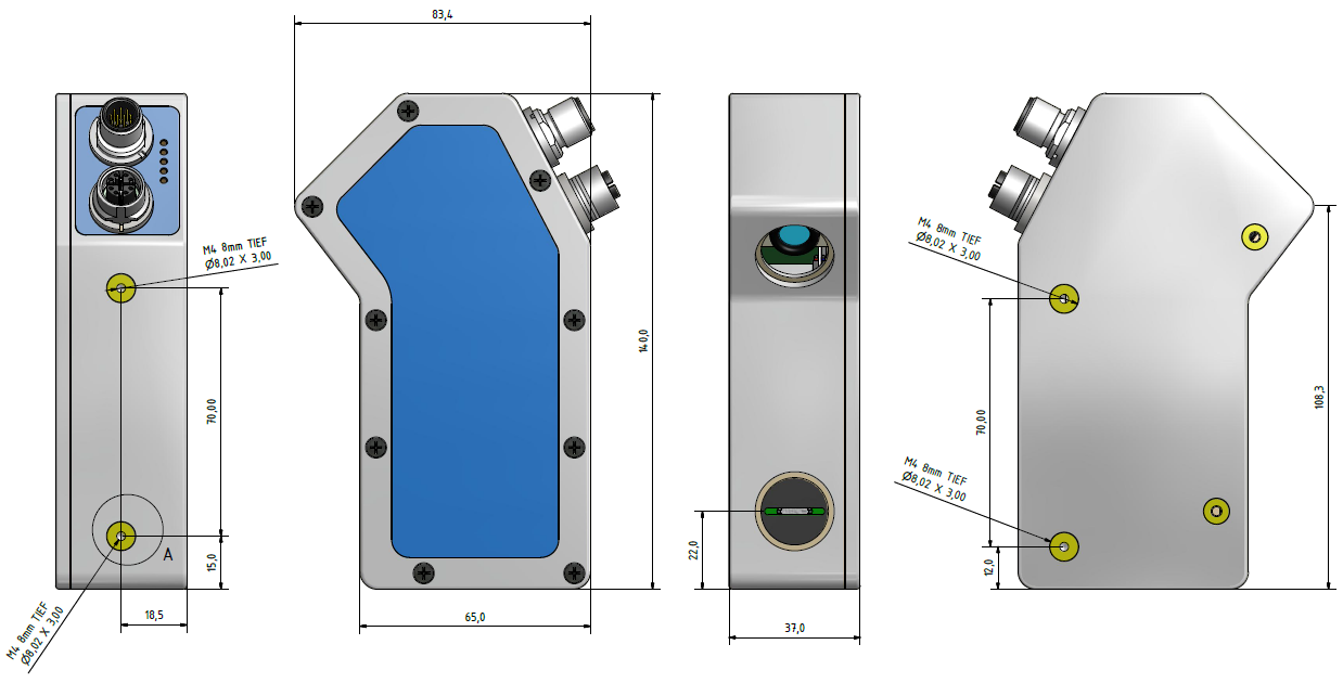
Dimensions of VC nano 3D Z Series - Regular model